Seeing the Invisible at NIST
Spring
2022
Building Blocks - Undergraduate Research and Outreach Projects
Seeing the Invisible at NIST
Joseph Tibbs, 2019 SPS Summer Intern and PhD Student, University of Illinois Urbana-Champaign
 How do we know what we know? In philosophy, this question is addressed in a field of study called epistemology. In the sciences, the nearest approximation of this would be metrology. Every measurement has inherent imprecision and bias, and metrologists seek to understand these errors and improve measurement technology. Microscopy overlaps heavily with these ideals and specifically seeks to create images of things that were previously invisible. My desire to learn about biological molecules at greater precision than ever before, and my background in physics and biochemistry, means I end up doing a lot of microscopy.
In the summer of 2019, I found myself immersed in a unique research environment in which metrology was the starting point and focus, with every other field of physics (and science as a whole) stemming from that perspective. The campus of the National Institute of Standards and Technology (NIST) is located just outside of Washington, DC, and I was stationed there as part of the SPS summer internship program. Other members of my cohort were exploring science policy on Capitol Hill, science communication at Physics Today, library science at the Niels Bohr Library & Archives, and engineering at NASA. Meanwhile, I was at NIST, a place where seeing the invisible is an everyday occurrence.
At NIST the goal of creating cutting-edge measurement technology mingles with the practical concern of ensuring that business runs smoothly and with well-defined and rigorously implemented standards. Standards underlie everything from civil engineering to the design of semiconductor chips. How do you ensure that building codes adequately protect against deadly fires? By studying the physics of fire using advanced simulations. How do you conduct quality control on computer chips? By finding defects before they get placed into devices.
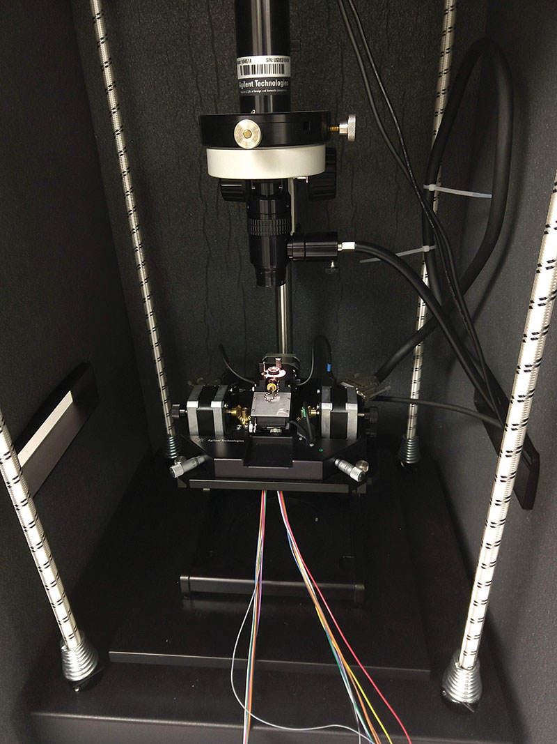
For those of us researching under Joe Kopanski, the leader of the Nanoscale Imaging Group at NIST, this meant working on a technology called electrostatic force microscopy (EFM). In most scanning-probe microscopy techniques, a vibrating cantilever with an atomically sharp tip scans over a surface at a distance of mere nanometers. The forces on the tip, resulting from miniscule changes in topography or surface properties, lead to a shift in resonant frequency that can be measured by sensitive electronics. Because the measurement is based on near-field interactions, subnanometer resolution is the result.
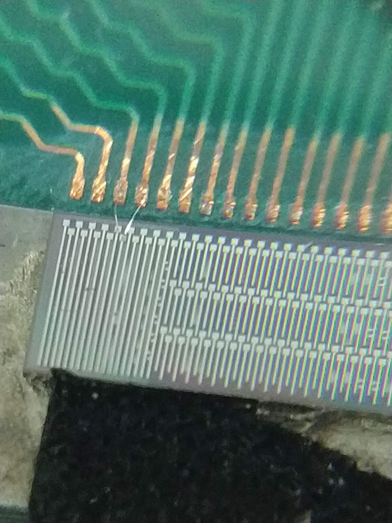
Specifically, our group wanted to adapt this technology to search for defects in embedded wiring in layered integrated circuit devices. Although these wires are covered by insulating material, electrostatic forces from applied voltages can still propagate a short distance and be picked up by the tip of the EFM machine. In the process of characterizing this machine, I learned about the physics of probe microscopy through both hands-on interactions with the machine and by building software simulations of the system.
It’s hard to collect a complete data set during a 10-week internship. Some would see this as a downside—if I didn’t publish a paper or generate visible results, what was the point? But if working at NIST taught me anything, it’s that what isn’t visible can be just as impactful. My senior thesis, which I completed the following year, relied on data taken on a scanning-probe microscope that just happened to be identical to the one used at NIST. The simulation tool I learned to use during the internship is commonly used in my current lab to help design new photonic materials.

At NIST I also had a long conversation with John Kasianowicz, a biophysicist, about science career paths and what it means to find your field. He encouraged me to never think of myself as being tied to a single field; he started in electrical engineering before working with biomolecules. When I took my qualifying exam last year as part of my PhD program, I had to give a presentation on two research papers, one of which was about a technology called nanopore sequencing. When I looked at the references of this paper, one entry stood out—a paper that provided the first experimental evidence of nanopore sequencing. The author: J. Kasianowicz.
Internships provide skills and experience relevant to your field of study, but they also broaden your horizons. All of science is interconnected, to much the same degree as the fields of microscopy and metrology are. The more connections you can make, both between pieces of information and between collaborators, the better. And, as in an integrated circuit, just because the connections are invisible doesn’t mean they aren’t important. //

Be an SPS Summer Intern!
The SPS summer internship program offers 10-week positions for undergraduate physics students in science research, education, and policy with various organizations in the Washington, DC, area. All internships include paid housing, a competitive stipend, support to attend a national physics meeting in the year following the internship, and transportation to and from Washington, DC.
To learn more, visit spsnational.org/programs/internships. Mark your calendar for summer 2023! The application deadline is January 16.
More from this department
Building Blocks - Undergraduate Research and Outreach Projects
