Monday, June 15, 2015
By:
Week three already? It feels like it was just yesterday that I was introduced to the fascinating world of MOSFETs (metal oxide semiconductor field-effect transistors) and now I am just waiting for the target substrate to be finished so I can start exfoliating the MoS2(Molybdenum Disulfide) flakes onto it. Remember how last week I wrote about gathering an electrostatic profile of a protein by sensing the electrostatic potential of each molecule that composes it? Well, there has been a slight change of plans, at least for the time that I will be here--this will eventually happen, but I will be gone by then (:/). Instead, I am going to look at the change in current that occurs when proteins attach to receptors.
The great thing about a MOSFET is that it requires a lot less current to turn on than a regular transistor. Typically, doped Si (Silicon) semiconductors are used in MOSFETs but in our case, we are going to use MoS2 as the semiconductor part of our device. We are going to exfoliate it onto our target silicon substrate, which is being developed right now and has two completely different things occurring on the front and back side. The back side has been etched away via the wet etching technique using KOH (Potassium Hydroxide) to create a small cave in the silicon wafer and the front side has alignment marks that were created using the photolithography process. The substrate needs to be etched a bit more to get rid of some of the protective layers that it currently has such as Si3N4(Silicon Nitride). The final step will be to grow a SiO2(Silicon Dioxide) layer on the front side. All of this is being accomplished by Jung-Joon Ahn, a graduate student. After the final step, we will be able to exfoliate the tiny MoS2 flakes onto the wafer and we will be looking for ones that are 10 nanometers thick and 10 to 20 microns (micrometers) in length and width. Once we obtain the desired flakes on the substrate, we will add the source, gate, and drain components to create our MOSFET. Receptors will be attached to the back side of the substrate and this side is the one that will be exposed to a biomolecule solution. When certain proteins attach to the receptors there is a transfer charge changing the charge density of MoS2, this then should allow us to see a particular change in current.
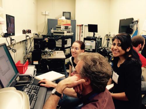
Now that I have given a glimpse of what the goals are for this summer, here is how I spent my week. I worked with AutoCAD drawing the source, gate, and drain terminals on a flake, really taking my time to learn this software. I analyzed the IV (current-voltage) data Dr. Suehle gave us to obtain the charge mobility of a MOSFET. I learned how to use the equipment for sourcing and measuring current and voltage of a MOSFET, which consisted of the SPA (Semiconductor Parameter Analyzer), the probe station, the optical microscope attached to the probe station, and the computer software to setup the parameters necessary to make a run. Once the MOSFET is finished, we will be using this equipment. Next week, I am hoping the substrate is finished and I can start the exfoliating process.

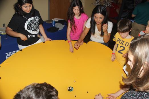
Outside of lab, I attended the YAE Hubble STEM Festival at STSI (Space Telescope Science Institute) with other SPS interns and staff. We had a lot of kids and parents come by our table. We set up a space-time warping demonstration by making use of a spandex sheet, flexible tubes, and marbles. The kids were so entertained with path the marbles made on their way to the massive object at the center. After the festival, we stopped at The Dizz restaurant for dinner. Sunday, I visited the National Cathedral with Aman. The cathedral is gorgeous, I loved the space window. I was taken away when I learned that it holds a lunar rock that was donated by the crew of Apollo 11! This just made the window look ever more perfect.
Veronica Martinez-Vargas

